The leading solution for AFM in SEM
The combination of complementary techniques is a key success factor for gaining new insights into the micro and nano worlds. AFSEM®, offered by GETec Microscopy, enables you to easily combine two of the most powerful analysis techniques available — AFM and SEM — to greatly extend your correlative microscopy and analysis possibilities.

“Constantly, applications and challenges arise for which the AFSEM is not only practical, but essential. That starts with direct correlation of specific particles or structures and ends with vacuum conditions as prerequisite, such as thermal measurements. Furthermore, the AFSEM accelerates the work-flow and therefore increases the efficiency for many studies.”

“The high spatial resolution of AFSEM, especially in Z direction, strongly stretched the application of our SEM. Combined with the high angle resolution of EBSD, the AFSEM becomes a powerful tool for the research of phase transformation.”

“What was really convincing to us is the huge versatility of this combination of an Atomic Force Microscope with our excellent optical microscope for our challenging materials and problems. We simply can use real life specimen without big preparation.”

“AFSEM® not only extends the resolution of our microscopes by an order of magnitude, it extends our measurement capabilities beyond topography concerning material composition.”

“Thanks to the AFSEM we can now perform in situ investigations in our FIB microscope, which were not possible before. Especially the possibility to immediately control the result of your nanofabrication experiment is a real benefit!”
In situ AFM analysis in your SEM

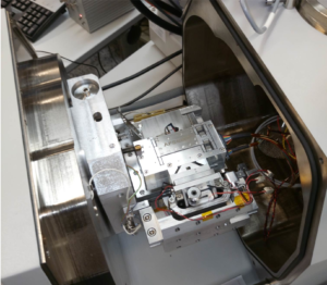
Integration of AFSEM® in a Zeiss Leo 982 SEM (left). SEM image of the in situ operation of the AFSEM® cantilever, scanning the sample surface (right). When alternating between AFM and SEM imaging, there is no need to transfer the sample or break the vacuum. With AFSEM® everything can be done inline!
The complimentary capabilities of AFM and SEM allow for unique characterization possibilities of your samples. AFSEM® lets you simultaneously image your sample with high resolution, create true 3D-topography representations, and accurately measure heights, distances and even material properties, all while maintaining the large SEM field of view to position your AFSEM® cantilever exactly where you want it. The optimized AFSEM® workflow (with practically no reduction of the SEM uptime) ensures highest possible effectiveness, while the powerful control software allows for optimized and intuitive measuring, system handling, and data analysis.
Correlative SEM-AFM analysis
For product or material analysis, it is often desirable to analyze a sample with multiple techniques and look for correlations between parameters. For imaging techniques like SEM and AFM this means one should make sure to analyze the exact same area! What easier way for correlative SEM-AFM analysis than performing the AFM measurement directly inside the SEM?

Correlative SEM and AFM analysis of unsupported graphene and graphene-related materials. In low-voltage SEM, a sample of unsupported graphene sheets can be screened to identify the presence of layers and their thickness (A). Areas of interest can then be imaged with higher resolution and better contrast using AFM (B+C).

SEM overview (A), SEM zoom (B), and correlative AFM imaging (C) of a scratched Gold surface measured in an FEI Quanta 600 FEG ESEM.
Compatible with most SEMs without impeding normal operation
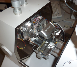
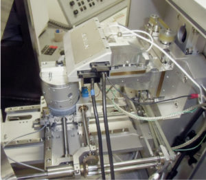
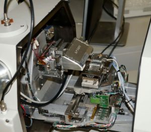
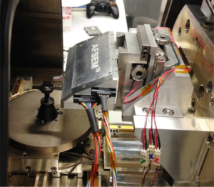

Examples of successful AFSEM® integrations (click on the individual images for details).
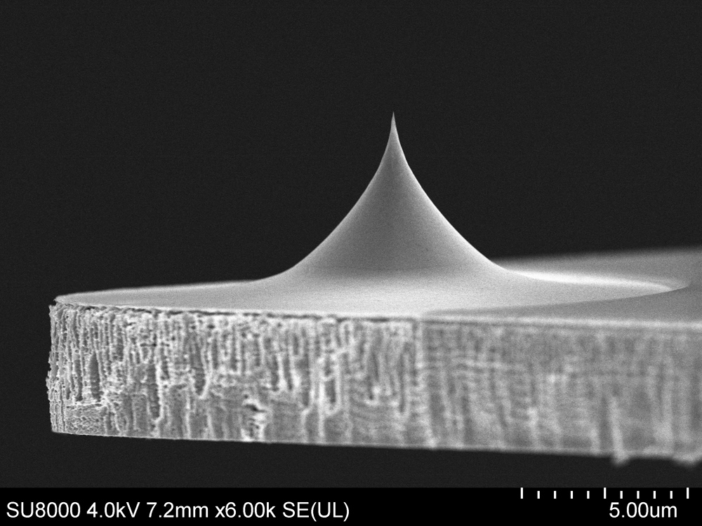
AFSEM® fits into most SEM or dual beam (SEM/FIB) systems: it is mounted directly on the door of the system chamber, leaving the stage unaltered. In addition, a slim tip-scanning design in combination with self-sensing cantilevers requires only 4.5 mm space between the pole shoe of the electron column and the sample. As a result, AFSEM® is compatible with a wide range of standard and optional stages, and can handle virtually any sample that fits the system chamber. This elegant design allows detection of sub-nanometer step heights in the SEM.
Many analysis techniques in parallel to AFM and SEM
Because the AFSEM® design maintains full SEM functionality, it works in combination with other standard SEM analysis techniques such as FIB, FEBID, and EDX.

Schematic representation and image of the non-obstructive integration of AFSEM® in SEM/Dual Beam systems, which allows many analysis techniques (e.g. FIB, FEBID, and EDX) in addition to AFM and SEM.
Because the sample is not scanned, also relatively heavy or specialized stages — for example for tensile stretching or nano-indentation — can be easily combined with AFSEM®.

AFSEM® and Deben 200N tensile stage installed in a Philips XL40 SEM (A). The SEM is used to localize the neck formation, quantify the degree of necking, and position the cantilever at the center of the neck (B). Surface roughness is quantified by AFM, and surface topology characterized in further detail (C).

AFSEM® and Hysitron PI85 SEM PicoIndenter® stage installed in a Zeiss Leo 982 SEM (A). The SEM is used to position the indenter tip and to measure the extent of topological changes after the indentation (B). The slip steps are quantified by AFM (C). For more information, please see our Nanoindentation analysis with AFSEM® application note.
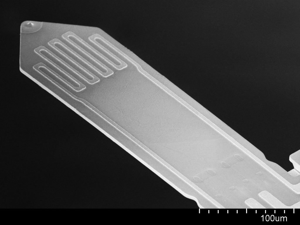
From the AFM side as well, multiple modes are available through specific self-sensing cantilevers, for example for Static and Dynamic Imaging, Phase Contrast, Force Spectroscopy, Force Modulation, and Conductive AFM, with more modes and cantilevers to follow. This for example enables the study of dose-dependent conductivity of Pt(C) after focused electron beam induced processing (FEBIP).
This constitutes the real power of AFSEM® and makes it the world leading solution for AFM in SEM.
Intuitive handling with self-sensing cantilever technology
AFSEM® offers maximum flexibility and intuitive positioning. The 3-axis coarse stage moves the cantilever into or out of the field of view of the SEM and positions the cantilever to an area of interest. The SEM stage moves the sample laterally for both AFSEM® and SEM. Vertically, AFM and sample are moved together, allowing you to safely move the sample up and down without crashing the AFM cantilever.
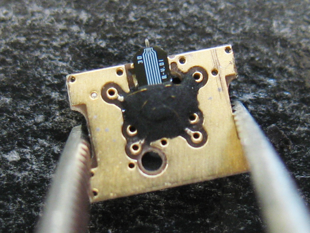
All cantilevers come pre-mounted on a standard connector that enables a fast tip exchange in less than 2 minutes, therefore greatly reducing the down-time of your system. Because of the self-sensing cantilever technology and fully automated cantilever alignment, the AFSEM® system is ready for operation immediately. The cantilevers are provided by our partner company SCL-Sensor.Tech. Fabrication GmbH.
AFSEM® components and accessories
- AFSEM® scan head
- AFSEM® toolkit (includes a selection of cantilevers)
- XYZ stage for AFSEM® scan head + SEM-specific adapter and feedthrough flange
- Controller, HV Amplifier, Computer (all in a rack housing) + Software
- AFSEM® cantilevers are available at SCL-Sensor.Tech
Free pre-sales consultancy from one of our experienced application scientists
Our experts will be pleased to discuss the demand of your application and analyze the possibilities of the AFSEM® integration into your existing equipment. We will offer a dedicated solution: hardware, software, installation, training, and after-sales support. This includes on-site and on-demand support, a wide choice of cantilevers, spare parts, and calibration service.

