
AFSEM® — AFM in-situ SEM

Two microscopes are better than one
GETec Microscopy offers innovative Atomic Force Microscopy solutions for seamless integration into existing host systems like Scanning Electron Microscopes. In partnership with our customers, we develop dedicated nano analysis tools based on pre-engineered modules.
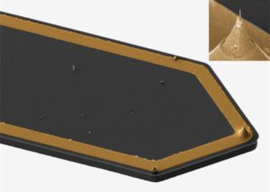
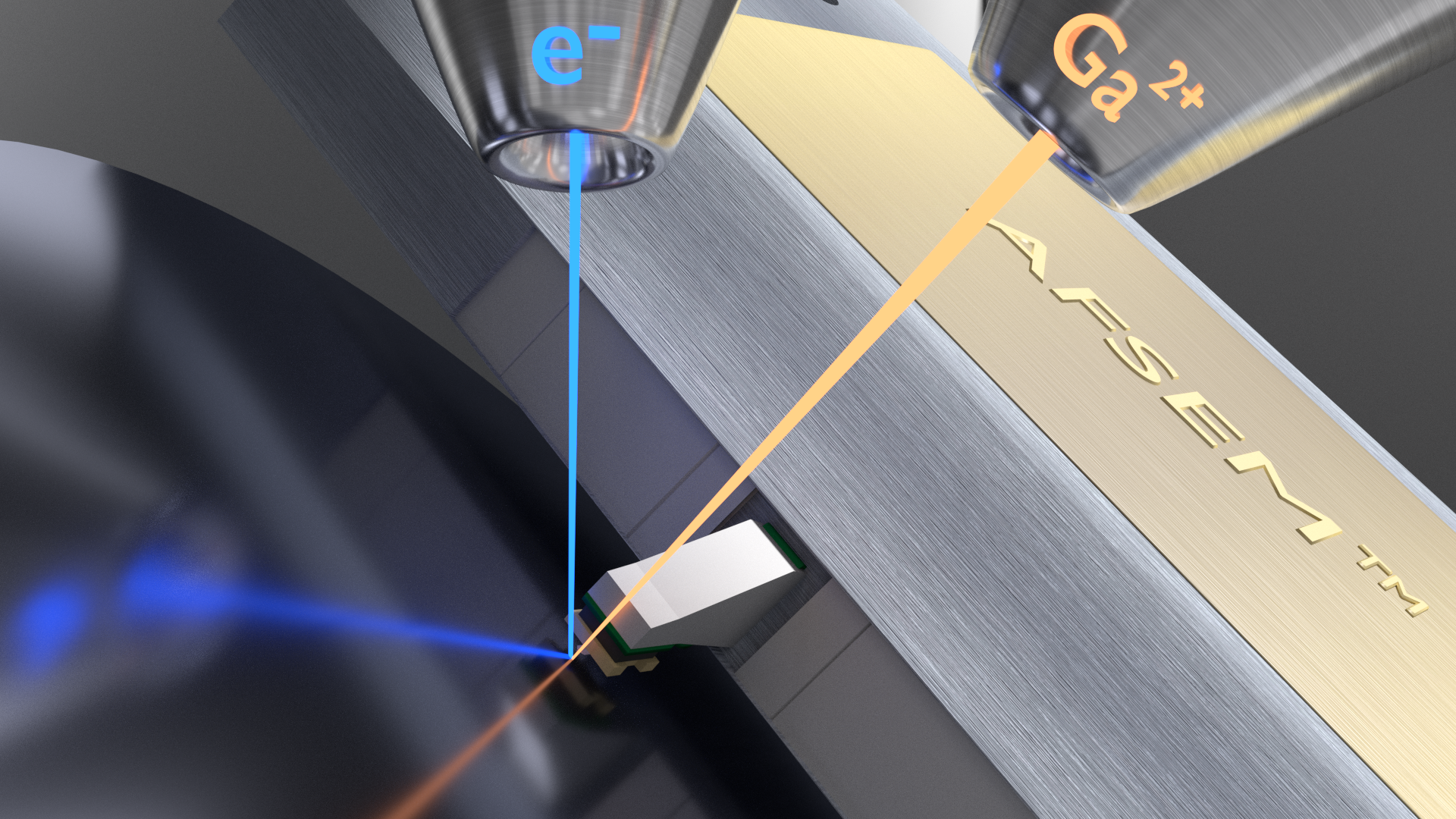
AFSEM® is an AFM by GETec Microscopy, designed for integration into an SEM or Dualbeam (SEM/FIB) microscope. It’s open access design allows to simultaneously operate SEM and AFM inside the SEM vacuum chamber. The complimentary image data of AFM and SEM enable unique characterization of your sample.
What is your Application?


Latest News

2019 June: MFM using AFSEM article in Spectrum magazine
The 3oth edition of the Spectrum magazine by Quantum Design LOT feautures the AFSEM. The article focuses on In situ Magnetic Force Microscopy (MFM) analysis of nanostructues using our product. Read article...

2019 June 18th: AFM in-situ SEM seminar Leatherhead, Surrey
Our partner Quantum Design UK and Ireland is hosting an AFM in-situ SEM seminar in Leatherhead, Surrey. GETec's Ernest Fantner will be present to tell you more about our AFSEM, its unique applications and what it is that makes it stand out from the rest. Furthermore, a live demo will take place, for you to see our product in action [...]

2019 June 12th-14th: 3rd EuFN Workshop in Dresden
Meet GETec at the 3rd Workshop of the European FIB Network in Dresden. Chris Schwalb and Stefan Hummel will be giving a presentation on in-situ correlative analysis of FIB-treated samples. Furthermore, feel more than free to ask any questions you might have regarding this novel analysis method and tool.
2019 July, 1-3: 20th Conference on Solid State Analysis in Vienna
Meet GETec at the 20th Conference on Solid State Analysis in Vienna next week! This year's special focus will be on "New Surfaces and Functional Layers – Functionalizing and Analyzing". On tuesday at 11:35 GETec's Chris Schwalb will be giving a presentation on In-Situ Correlative AFM/SEM/FIB analysis of FIB-treated samples. Furthermore, we would be happy to welcome you at our [...]
AFSEM® users about our product…

“Constantly, applications and challenges arise for which the AFSEM is not only practical, but essential. That starts with direct correlation of specific particles or structures and ends with vacuum conditions as prerequisite, such as thermal measurements. Furthermore, the AFSEM accelerates the work-flow and therefore increases the efficiency for many studies.”

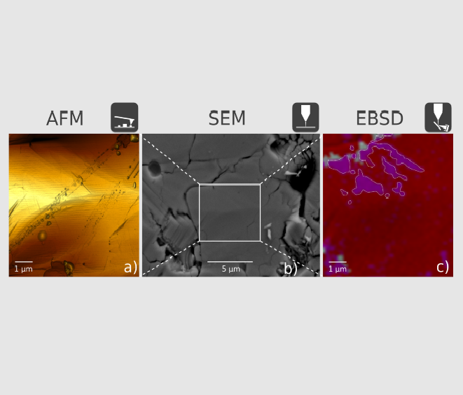
“The high spatial resolution of AFSEM, especially in Z direction, strongly stretched the application of our SEM. Combined with the high angle resolution of EBSD, the AFSEM becomes a powerful tool for the research of phase transformation.”

“What was really convincing to us is the huge versatility of this combination of an Atomic Force Microscope with our excellent optical microscope for our challenging materials and problems. We simply can use real life specimen without big preparation.”

“AFSEM® not only extends the resolution of our microscopes by an order of magnitude, it extends our measurement capabilities beyond topography concerning material composition.”

“Thanks to the AFSEM we can now perform in situ investigations in our FIB microscope, which were not possible before. Especially the possibility to immediately control the result of your nanofabrication experiment is a real benefit!”